The Silicon Sovereignty Blueprint: A Comprehensive Guide on India’s Semiconductor Ambitions
Semiconductors have transcended their status as microelectronic parts to become the strategic foundation of 21st-century geopolitics, national defense, and industrial power. Often characterized as the “new oil” of the modern digital era, these micro-scale chips dictate leadership in artificial intelligence, aerospace, telecommunications, and automotive manufacturing.
Recognizing that heavy dependence on global supply lines presents severe economic and security vulnerabilities, the Government of India has embarked on an ambitious policy campaign. Anchored by the initial India Semiconductor Mission (Semicon 1.0) with an outlay of ₹76,000 crore, and further reinforced by the approval of Semicon 2.0 with a dedicated outlay of ₹1,27,500 crore, the nation is actively pivoting from being merely a high-volume consumer of electronics to an indispensable, trusted manufacturing and innovation node in global value networks.
This comprehensive study guide and analytical report breaks down the scientific principles, industrial complexities, international supply dynamics, policy mechanisms, and multi-phased roadmap defining India’s semiconductor journey.
1. Semiconductor Fundamentals: Physics, Materials, and the Transistor
To understand the economics and geopolitics of microchips, one must first examine the solid-state physics that makes digital computing possible.
Electrical Conductivity and the Semiconductor State
All physical materials fall across a spectrum of electrical conductivity:
-
Conductors: Materials such as copper and aluminum possess high electron mobility, allowing electrical charges to flow freely with minimal resistance.
-
Insulators: Substances such as glass, quartz, and rubber tightly bind their valence electrons, preventing current from passing under normal conditions.
-
Semiconductors: Elements such as silicon (Si) and germanium (Ge) feature an intermediate electrical conductivity that can be precisely altered, switched, and modulated through thermal, optical, or chemical manipulation.
[Insulators (e.g., Glass)]  <---  [SEMICONDUCTORS (e.g., Silicon)]  --->  [Conductors (e.g., Copper)]
      (Zero Current)                 (Precisely Modulated Current)             (Free Flow)
The Dominance of Silicon
Silicon remains the bedrock of modern microelectronics due to three unique advantages:
-
Natural Abundance: Derived from silica sand, silicon is the second most abundant element in the Earth’s crust, guaranteeing raw material security.
-
Ultra-Purification Capability: Industrial chemical refining processes allow metallurgical-grade silicon to be converted into electronic-grade silicon (EGS) with purity levels exceeding 99.9999999% (“nine-nines”).
-
Stable Native Oxide: Silicon easily forms silicon dioxide ($SiO_2$), a resilient insulating layer critical for lithographic patterning and surface passivation.
The Chemistry of Doping: Engineering P-Type and N-Type Regions
Pure silicon forms a uniform crystal lattice where each atom shares four covalent bonds with its neighbors, leaving zero free charge carriers at low temperatures. To control electricity, engineers introduce minute quantities of foreign atoms in a process known as doping:
-
N-Type Semiconductor (Negative Charge Donors): Introducing pentavalent impurities (e.g., phosphorus or arsenic) introduces extra conduction electrons into the lattice, boosting electron concentration.
-
P-Type Semiconductor (Positive Charge Acceptors): Introducing trivalent impurities (e.g., boron or gallium) creates “holes”—vacancies in covalent bonds that behave as positive charge carriers.
The Transistor: The Microscopic Binary Switch
By interfacing doped p-type and n-type silicon regions, engineers construct the transistor (most commonly a Field-Effect Transistor, or FET).
-
Source: the point of entry for charge carriers into the channel.
-
Drain: The terminal where charge carriers leave the channel.
-
Gate: The regulatory terminal positioned above the channel, separated by a thin dielectric insulator.
-
Silicon Substrate: The structural foundation supporting the transistor architecture.
Applying a specific voltage to the gate terminal creates an electric field that turns the conductive channel between source and drain ON (current flows, denoting binary 1) or OFF (current ceases, denoting binary 0). Modern microchips pack tens of billions of these microscopic switches onto a sliver of silicon the size of a fingernail, operating at gigahertz frequencies to execute complex mathematical calculations, run AI algorithms, store data, and process signals.
2. Industry Decoupling: Fabless Chip Design vs. Foundry Fabrication
The semiconductor industrial model is divided into two distinct, highly specialized operational models: Chip Design (Fabless) and Wafer Manufacturing (Fab).
+---------------------------------------------------------------------------------------------------+
|                                  THE SEMICONDUCTOR VALUE CHAIN                                    |
+--------------------+--------------------+--------------------+--------------------+---------------+
| 1. Design          | 2. Front-End Fab   | 3. Packaging       | 4. Final Testing   | 5. End Market |
| (EDA, Architecture)| (Cleanrooms, Litho)| (Dicing, Assembly) | (Burn-in, QA)      | (Auto, AI)    |
+--------------------+--------------------+--------------------+--------------------+---------------+
The Fabless Paradigm
Fabless companies focus exclusively on the conceptual, architectural, and logical design of the integrated circuit without operating capital-intensive physical production plants.
-
Functional Definition: Determining the functional target of the chip—whether a central processing unit (CPU), graphics processor (GPU), neural processing unit (NPU), application-specific integrated circuit (ASIC), or power management IC.
-
Architectural Engineering: Routing billions of logical paths, balancing power dissipation, optimizing clock speeds, and minimizing latency.
-
EDA Software: Utilizing electronic design automation (EDA) software suites (from providers such as Synopsys, Cadence, and Siemens EDA) to simulate and verify silicon physics virtually.
-
Output File: The final deliverable is an industry-standard layout file (such as GDSII or OASIS format) containing the physical geometry of every circuit layer.
-
Leading Fabless Firms: NVIDIA, Qualcomm, AMD, MediaTek, and Apple.
The Pure-Play Foundry Paradigm
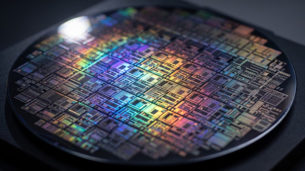
A semiconductor fabrication plant (“fab”) takes the digital GDSII blueprint and physically constructs it on an ultra-pure circular silicon wafer through hundreds of sequential chemical, thermal, and optical steps:
-
Wafer Preparation: Silicon ingots are grown, sliced into thin discs, and polished to atomic flatness.
-
Photolithography: Light-sensitive photoresist is applied, exposed to extreme ultraviolet (EUV) or deep ultraviolet (DUV) light through optical reticles (masks), transferring the microscopic circuit pattern.
-
Deposition: Nanometer-thin films of conductors, semiconductors, or dielectric materials are deposited using chemical vapor deposition (CVD) or physical vapor deposition (PVD).
-
Etching: Liquid chemicals (wet etching) or ionized gas plasmas (dry etching) strip away unprotected material, carving the transistor layout.
-
Ion Implantation (Doping): High-energy ion beams embed dopant atoms into exact regions of the exposed silicon.
Comparative Overview: Design vs. Fabrication
| Dimension | Chip Design (Fabless) JPG | Chip Manufacturing (Foundry / Fab) JPG+ 1 |
| Core Asset |
Intellectual Property (IP), Human Capital, EDA Licenses |
Physical Cleanrooms, Precision Machines, Chemical Lines |
| Capital Intensity |
Moderate (Predominantly OpEx for R&D and Software) |
Extreme (Billions of dollars in initial CapEx and tool maintenance) |
| Gestation Period | 18 to 36 months to produce a tape-out design |
3 to 5 years to build, qualify, and ramp a fab facility |
| Key Risk | Architectural flaws, time-to-market delays, IP theft |
Yield degradation, power interruptions, supply chain shortages, node obsolescence |
| India’s Stance |
Controls nearly 20% of global chip design talent |
Nascent stage; actively building domestic manufacturing capacity |
3. The Engineering Anatomy of a Mega-Fab: Why Manufacturing is Difficult
A modern semiconductor fab is among the most structurally and operationally complex industrial facilities ever built. Constructing and sustaining a commercial fab requires overcoming extreme engineering challenges:
+-----------------------------------------------------------------------------------+
|                        THE NINE PILLARS OF FAB COMPLEXITY                         |
+----------------------------------+------------------------------------------------+
| 1. Immense Capital Investments   | Multi-billion-dollar outlays ($10B+ per plant) |
| 2. Nanometer Precision           | Processing down to atomic dimensions (<5nm)    |
| 3. Ultra-Clean Manufacturing     | ISO Class 1 cleanrooms; zero dust tolerance    |
| 4. Monopolized Machinery         | Critical reliance on EUV lithography systems   |
| 5. High-Purity Raw Materials     | 99.9999999% pure chemicals and specialty gases |
| 6. Uninterrupted Utilities       | Gigawatt-scale power and millions of gal/day   |
| 7. Specialized Manpower          | Top-tier material scientists and process eng.  |
| 8. Rapid Node Obsolescence       | Heavy recurring CapEx every 2 to 3 years       |
| 9. Ecosystem Dependency          | Synergistic web of co-located suppliers        |
+----------------------------------+------------------------------------------------+
-
Extreme Capital Demands: Building a single advanced-node fabrication plant costs between $10 billion and $20 billion (₹80,000 to ₹1,60,000+ crore). Financial viability requires running equipment at 85–95% capacity utilization 24/7.
-
Nanometer-Scale Tolerances: Transistor features are measured in nanometers ($1\text{ nm} = 10^{-9}\text{ meters}$). For scale, a human hair is roughly 80,000 to 100,000 nanometers wide. A single misaligned layer at the atomic scale will ruin thousands of circuits.
-
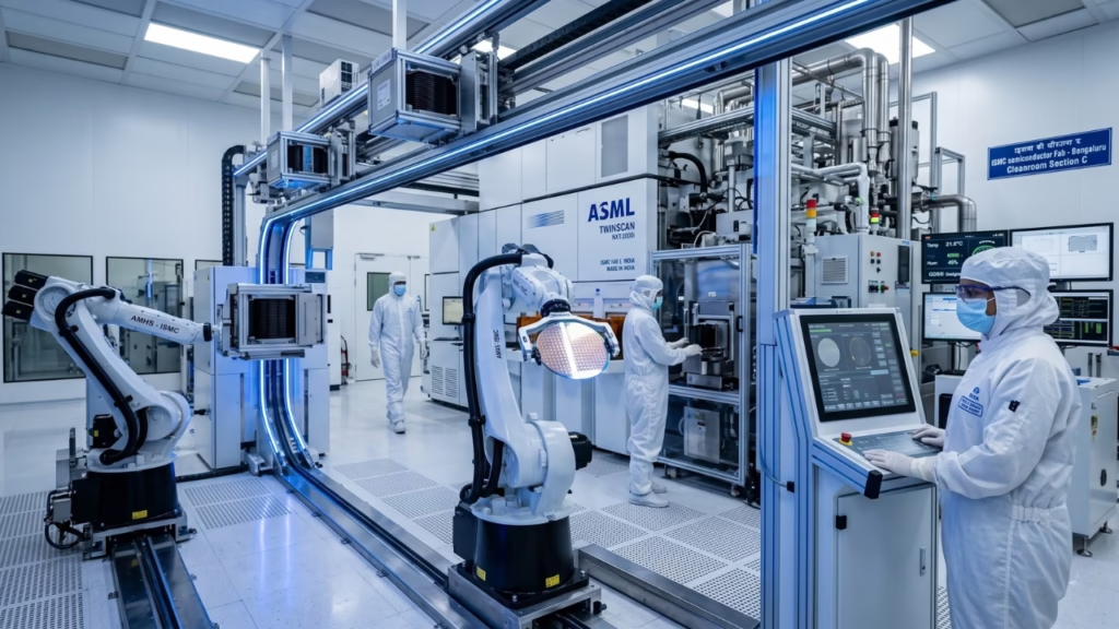
Ultra-Clean Environments: Advanced fabs operate ISO Class 1 cleanrooms containing fewer than 10 particles of 0.1-micron size per cubic meter of air. Technicians wear completely sealed positive-pressure cleanroom suits (“bunny suits”), as a single skin cell or speck of dust ruins an entire wafer.
-
Monopolized Specialized Tooling: A fab relies on high-end machinery: extreme ultraviolet (EUV) scanners, chemical mechanical planarization (CMP) tools, and plasma etchers. Photolithography tools utilize laser systems operating under vacuum, produced by only a handful of vendors worldwide.
-
Stringent Infrastructure Demands: A large-scale fab requires 50 to 100 megawatts of continuous, uninterruptible electrical power without micro-second voltage fluctuations, alongside millions of liters of Ultra-Pure Water (UPW) daily.
-
Recurring Capital Expenditure: Process nodes advance every few years. A fab that fails to invest continuously in node transitions risks technological obsolescence within a decade.
4. Packaging, Assembly, and the Advanced Heterogeneous Revolution
Fabricating silicon circuitry on a wafer is only the front-end phase of the semiconductor lifecycle; raw wafers cannot be mounted directly onto circuit boards.
[Raw Fabricated Wafer] ---> [Wafer Dicing] ---> [Die Assembly] ---> [Substrate Packaging] ---> [Testing/QA] ---> [Final Packaged Chip]
From Wafer to Packaged Die: The ATMP/OSAT Workflow
The backend sequence is executed by ATMP (Assembly, Testing, Marking, and Packaging) or OSAT (Outsourced Semiconductor Assembly and Test) providers:
-
Wafer Dicing: A diamond saw or high-precision laser slices the completed wafer into individual microchips, known as dies.
-
Assembly and Die Attach: The functioning die is bonded to a supporting lead frame or package substrate.
-
Interconnection: Microscopic gold, copper, or aluminum wire bonds, or lead-free solder micro-bumps, connect the die’s input/output pads to the substrate.
-
Encapsulation (Packaging): The delicate silicon die is hermetically sealed within an epoxy resin or ceramic shell to protect it from thermal stress, oxidation, and physical impact.
-
Final Testing: Every packaged unit undergoes automated electrical, thermal, and functional burn-in tests to identify manufacturing defects before final distribution.
Advanced Packaging and Heterogeneous Integration
As traditional transistor miniaturization approaches physical limits (known as the slowing of Moore’s Law), the global microelectronics industry is pivoting toward Advanced Packaging:
-
Chiplet Architectures: Rather than manufacturing a massive, monolithic silicon die where all components (CPU cores, memory, graphics, I/O) share a single piece of silicon, designers split functions into smaller, modular chiplets.
-
2.5D and 3D Stacking: Chiplets are mounted side-by-side on silicon interposers (2.5D) or stacked vertically using Through-Silicon Vias (TSVs) (3D).
-
High-Bandwidth Memory (HBM): Memory stacks are integrated directly alongside AI processors via silicon interposers, bypassing circuit board latency and reducing power consumption.
India’s Tactical Window in Packaging
Establishing an OSAT/ATMP ecosystem presents lower entry barriers than building leading-edge fabrication facilities. Capital outlays run in hundreds of millions of dollars rather than tens of billions, commissioning schedules are shorter, and labor utilization is higher.
By securing major OSAT investments (such as the Micron facility in Sanand, Gujarat, and the Tata Electronics OSAT facility in Morigaon, Assam), India is establishing immediate physical integration into the global electronics supply chain.
5. The Interdependent Global Supply Chain: One Chip, Many Countries
The modern semiconductor industry is the most globally distributed, interdependent manufacturing network in human history. No single sovereign nation possesses a completely self-contained, end-to-end semiconductor ecosystem.
+----------------------------------------------------------------------------------------------------+
|                           THE GLOBAL SEMICONDUCTOR INTERDEPENDENCY MAP                             |
+----------------------+-----------------------------------------------------------------------------+
| United States        | EDA Software, Core IP, Chip Architecture, Advanced Logic Design, Equipment  |
| Taiwan               | World-Leading Pure-Play Foundry Capacity, Sub-5nm Process Nodes (TSMC)      |
| South Korea          | Global Memory Production Dominance (DRAM, 3D-NAND Flash - Samsung, SK Hynix)|
| Netherlands          | Monopolistic Precision Photolithography Systems (ASML EUV Scanners)         |
| Japan                | Silicon Wafers, Critical Photoresists, Etching Chemicals, Ultra-Pure Gases  |
| China                | High-Volume Assembly, Legacy Nodes, Extensive Electronics Integration Supply|
| India (Emerging)     | Premier Design Talent, Expanding ATMP/OSAT Hub, Maturing Production Units   |
+----------------------+-----------------------------------------------------------------------------+
Key National Specializations
-
United States: Leads in chip design, algorithmic architecture, electronic design software, and high-end processing IP. Companies like Applied Materials, Lam Research, and KLA also make it an indispensable player in fabrication equipment.
-
Taiwan: The epicenter of contract foundry fabrication. Through Taiwan Semiconductor Manufacturing Company (TSMC), Taiwan manufactures more than 60% of all semiconductors and over 90% of the world’s sub-5nm advanced chips.
-
South Korea: Commands over 60% of the worldwide memory market. Samsung and SK Hynix lead global production of dynamic random-access memory (DRAM) and NAND flash memory.
-
The Netherlands: Holds an absolute monopoly in extreme ultraviolet (EUV) photolithography through ASML. Without ASML’s optical systems, producing chips below the 7nm node is impossible.
-
Japan: Controls upstream chemical and physical inputs. Japanese suppliers produce electronic-grade silicon wafers, specialized fluorinated polyimides, photoresists, and ultra-high-purity hydrogen fluoride.
-
China: The largest overall market for semiconductors, with an unmatched electronics assembly ecosystem. China is investing heavily in domestic self-reliance, with dominant capacity in mature nodes ($\ge 28\text{nm}$).
This extreme specialization creates fragile single-point chokepoints. Geopolitical flashpoints, maritime blockades, natural disasters, or export controls can disrupt downstream industrial production globally within weeks. India’s strategy is not isolationist autarky, but becoming an essential, trusted node within this global network.
6. India’s Strategic Imperatives: National Security, Economics, and Tech Sovereignty
India’s drive to develop domestic semiconductor production is rooted in national defense, macroeconomic resilience, and technological sovereignty.
                             +-----------------------------------+
                             |    INDIA'S STRATEGIC TRIAD        |
                             +-----------------+-----------------+
                                               |
         +-------------------------------------+-------------------------------------+
         |                                     |                                     |
+--------v-------------------+    +------------v---------------+    +----------------v---------------+
| 1. NATIONAL SECURITY       |    | 2. ECONOMIC AUTONOMY       |    | 3. FUTURE TECHNOLOGIES         |
| Uncompromised defense chips|    | Mitigate import deficits   |    | Sovereign hardware for AI,     |
| and tamper-proof telecom   |    | and insulate local sectors |    | 5G/6G, and EV transitions      |
+----------------------------+    +----------------------------+    +--------------------------------+
1. National Security and Defense Autonomy
Modern defense platforms depend entirely on hardened, reliable electronics:
-
Radar arrays, guided missile tracking systems, tactical communications, and electronic warfare suites require specialized semiconductors.
-
Relying on foreign commercial foundries exposes critical military hardware to supply cutoffs during hostilities, unauthorized hardware backdoors, and state-sponsored espionage.
-
Domestic fabs guarantee sovereign control over secure silicon components running India’s strategic defense systems.
2. Reducing Import Dependence and Economic Exposure
India’s electronics consumption is growing rapidly, with chip imports forming a major share of the nation’s import bill. Without domestic production, this import dependence leaves key manufacturing sectors exposed:
-
The 2020–2022 global chip shortage halted automotive assembly lines across India, idling plants and showing that a lack of $2 microcontrollers can stall vehicles worth tens of thousands of dollars.
-
Domestic chip production secures key industrial sectors (automotive, electronics, industrial automation, telecommunications) against overseas factory shutdowns and volatile supply chains.
3. Powering Next-Generation Technologies
Technological leadership across the next two decades depends on specialized hardware architectures:
-
Artificial Intelligence: Large language models and computer vision platforms require high-performance compute accelerators.
-
Telecommunications: National rollouts of 5G and research into 6G networks require high-frequency RF transceiver chips and baseband processors.
-
Electric Vehicles (EVs): Transitioning to green transportation requires silicon carbide (SiC) and gallium nitride (GaN) compound semiconductors for motor inverters, power conversion, and battery management.
-
Smart Energy Grids: Decentralized renewable solar and wind systems require dedicated micro-inverters and power distribution chips.
7. Policy Architecture: Semicon India 1.0, 2.0, and Incentive Frameworks
To position India as a global manufacturing hub, the Union Government launched a comprehensive industrial policy suite backed by financial and regulatory support.
+----------------------------------------------------------------------------------------------------+
|                         INDIA'S SEMICONDUCTOR POLICY TIMELINE & SCOPE                              |
+----------------------------+-----------------------------------------------------------------------+
| Semicon 1.0 (2021)         | ₹76,000 Crore initial financial outlay                   |
| Important Support Systems  | 50% Fiscal Capital Support for Fabs and Packaging (Pari-Passu basis)    |
| Projects Approved(until2026)|Twelve Manufacturing & Packaging Facilities(planned capex of around ₹1.64 lakh cr)|
| Semicon 2.0 (July 2026)    | ₹1,27,500 Crore expanded outlay targeting deep-tech integration[cite: 1]|
| Strategic Expansion Areas  | Equipment tooling, chemical inputs, compound semis, EDA IP design[cite: 1]|
+----------------------------+-----------------------------------------------------------------------
Key Pillars of the Incentive Ecosystem
-
Direct Capital Support: The central government provides up to 50% financial support on a pari-passu basis for setting up silicon fabs, display fabs, compound semiconductor facilities, and ATMP/OSAT units. State governments often supplement this with additional 20–25% subsidies, land concessions, and subsidized utility tariffs.
-
Design-Linked Incentive (DLI) Scheme: Provides financial reimbursement and access to high-end EDA tool licenses for domestic startups, micro, small, and medium enterprises (MSMEs) working on indigenous chip design.
-
Modernizing Infrastructure: Establishing specialized Electronics Manufacturing Clusters (EMCs) equipped with plug-and-play utilities, high-purity water plants, dedicated power substations, and customs-bonded logistics corridors.
-
Workforce Development: Partnerships across hundreds of academic institutions to modernize curricula, train VLSI engineers, and develop practical expertise in cleanroom protocols and process engineering.
8. Structural Challenges and India’s Strategic Roadmap (1 to 15 Years)
Despite strong policy momentum, building a domestic semiconductor ecosystem is a multi-decade effort facing real structural challenges:
Structural Headwinds
-
Resource and Utility Constraints: Fabs require uninterrupted electricity and vast quantities of treated water. Maintaining these utility standards across industrial zones demands consistent, high-level operational execution.
-
Ecosystem Scale: A fab cannot operate in isolation; it depends on an ecosystem of gas purifiers, quartz tube suppliers, wafer suppliers, and chemical recyclers. Building this localized supply network takes years.
-
Global Subsidies Competition: The United States (US CHIPS Act), the European Union (EU Chips Act), Japan, and China are all offering tens of billions of dollars in subsidies to secure their own domestic manufacturing footprints.
-
Workforce Specialization: While India has abundant digital chip design talent, it faces a shortage of chemical, process, and material science engineers with hands-on fab experience.
The Phased Implementation Roadmap
+---------------------------------------------------------------------------------------------+
|                                THE MULTI-TIER ROADMAP                                       |
+--------------------------+------------------------------------------------------------------+
| Phase 1: Near-Term       | Rapid project execution, completing approved OSAT/ATMP and fabs, |
| (1–3 Years)              | solidifying infrastructure, and targeted workforce skilling.     |
+--------------------------+------------------------------------------------------------------+
| Phase 2: Medium-Term     | Expanding domestic design IP, scaling compound semiconductors,   |
| (3–7 Years)              | and integrating deeply into commercial electronics value chains. |
+--------------------------+------------------------------------------------------------------+
| Phase 3: Long-Term       | Leading-edge R&D, advanced nodes (<5nm), domestic lithography/   |
| (7–15 Years)             | materials, and high-volume sovereign manufacturing leadership.   |
+--------------------------+------------------------------------------------------------------+
1. Near-Term Priorities (Years 1 to 3)
-
Fast-Track Project Execution: Complete construction and commercial ramp-ups for all approved facilities under Semicon 1.0 on schedule.
-
Utility Guarantees: Ensure zero-defect utility infrastructure (water, electricity, waste handling) across primary semiconductor manufacturing clusters.
-
Foundational Talent Pipelines: Roll out specialized training curricula across premier engineering institutes to supply qualified technicians and process engineers.
2. Medium-Term Milestones (Years 3 to 7)
-
Domestic Supply Chain Development: Localize production of specialty chemicals, electronic-grade gases, and key consumable materials to reduce input risks.
-
Expand Commercial Design IP: Leverage the DLI scheme to establish homegrown fabless champions creating Indian-owned intellectual property for automotive, defense, and IoT markets.
-
Integrate Into Global Value Chains: Transition approved OSAT and mature-node fab plants into trusted suppliers for international consumer, enterprise, and automotive firms.
3. Long-Term Vision (Years 7 to 15)
-
Advanced Node Expansion: Transition manufacturing from legacy nodes (28nm, 40nm, 65nm) toward sub-7nm and sub-3nm processes for high-performance computing.
-
Compound Semiconductor Leadership: Establish major production hubs for Gallium Nitride (GaN) and Silicon Carbide (SiC) to supply global renewable power and EV markets.
-
Global Node Status: Establish India as a reliable, indispensable anchor in the international technology landscape, backing economic security and technical sovereignty.
9. Key Examination and Policy Takeaways
-
Definition & Core Function: A semiconductor’s conductivity sits between a conductor and an insulator. Transistors function as microscopic binary switches controlling electron flow via source, drain, and gate terminals.
-
Fabless vs. Foundry: Chip design requires software engineering, EDA tools, and architectural IP. Fabrication is an ultra-clean, capital-intensive manufacturing process requiring sub-nanometer physical precision.
-
Packaging as an Entry Point: Advanced 2.5D/3D packaging and ATMP/OSAT provide a faster, cost-effective route to integrate into global supply chains while bypassing traditional transistor scaling bottlenecks.
-
Interdependent Global Network: No nation is entirely self-sufficient in semiconductors. Success requires building trusted, resilient partnerships across key international nodes.
-
Strategic Imperatives: Securing domestic chip capacity safeguards defense infrastructure, insulates national industries from external supply shocks, and underpins growth in next-generation fields like AI, 5G/6G, and EVs.
-
Government Support: The combined outlays of Semicon 1.0 (₹76,000 crore) and Semicon 2.0 (₹1,27,500 crore) combine capital subsidies, design incentives, and infrastructure development to build a durable domestic ecosystem[cite: 1, 8].
Developing a self-reliant semiconductor ecosystem is a complex, long-term national endeavor requiring persistent capital investment, clear policies, and close collaboration between government, industry, and academia. By pairing its established chip design strengths with targeted investments in packaging, infrastructure, and fabrication, India is laying the foundation for long-term technological resilience and economic growth.